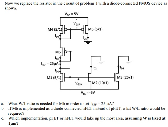
Now we replace the resistor in the circuit of problem 1 with a diode-connected PMOS device as shown
The Correct Answer and Explanation is:
Here is the correct answer.
To solve this problem, we must assume typical process parameters for the MOSFETs, as they are not provided. Let’s assume the following values for a standard CMOS process, ignoring channel-length modulation (λ=0):
- Electron mobility parameter, k’n = μnCox = 100 µA/V²
- Hole mobility parameter, k’p = μpCox = 50 µA/V²
- NMOS threshold voltage, Vtn = 0.7 V
- PMOS threshold voltage, Vtp = -0.7 V
All transistors in the reference leg carry I_REF = 25 µA and are assumed to be in saturation.
a. What W/L ratio is needed for M6 in order to set I_REF = 25 µA?
The total voltage drop across the reference leg is V_DD – V_SS = 5V – (-5V) = 10V. This voltage is distributed across the three series-connected transistors M4, M6, and M1. Using Kirchhoff’s Voltage Law:
V_DD – V_SS = V_SG4 + V_SG6 + V_GS1 = 10V
First, we find the gate-source voltages for M1 and M4 using the saturation current equation I_D = ½ * k’ * (W/L) * (V_GS – V_t)²:
- For M1 (NMOS): 25µA = ½ * (100 µA/V²) * (5/1) * (V_GS1 – 0.7V)², which gives V_GS1 ≈ 1.016 V.
- For M4 (PMOS): 25µA = ½ * (50 µA/V²) * (5/1) * (V_SG4 – 0.7V)², which gives V_SG4 ≈ 1.147 V.
Now, we find V_SG6 from the KVL equation:
V_SG6 = 10V – V_GS1 – V_SG4 = 10V – 1.016V – 1.147V = 7.837 V.
Finally, we calculate the W/L ratio for the pFET M6:
25µA = ½ * (50 µA/V²) * (W/L)6 * (7.837V – 0.7V)²
(W/L)6 = 25 / [25 * (7.137)²] = 1 / 50.94 ≈ 0.0196
b. If M6 is implemented as a diode-connected nFET instead of pFET, what W/L ratio would be required?
If M6 is an nFET, for it to conduct current from M4 to M1, its drain (higher potential) must connect to M4’s drain and its source (lower potential) to M1’s drain. For it to be diode-connected, its gate must be tied to its drain. Therefore, V_G6 = V_D6. The voltage at M6’s drain is V_D4, and the voltage at its source is V_D1.
- V_D4 = V_DD – V_SG4 = 5V – 1.147V = 3.853V
- V_D1 = V_SS + V_GS1 = -5V + 1.016V = -3.984V
The gate-source voltage for the nFET M6 is V_GS6 = V_G6 – V_S6 = V_D4 – V_D1 = 3.853V – (-3.984V) = 7.837V.
Now we calculate the required W/L ratio for the nFET M6:
25µA = ½ * (100 µA/V²) * (W/L)6 * (7.837V – 0.7V)²
(W/L)6 = 25 / [50 * (7.137)²] = 0.5 / 50.94 ≈ 0.0098
c. Which implementation, pFET or nFET, would take up the most area, assuming W is fixed at 1µm?
The area of a transistor is approximately A = W × L. Since W is fixed at 1µm, the area is directly proportional to the channel length L. The length can be expressed as L = W / (W/L). This means the implementation with the smaller W/L ratio will require a larger channel length L, and therefore will occupy more area.
Comparing the two results:
- (W/L)pFET ≈ 0.0196
- (W/L)nFET ≈ 0.0098
Since (W/L)nFET is smaller than (W/L)pFET, the nFET implementation will have a larger channel length and would take up the most area.