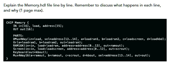
Explain the Memory.hdl file line by line. Remember to discuss what happens in each line, and why (1 page max). CHIP Memory { IN in[16], load, address[15]; OUT out[16]; PARTS: DMux4Way(in=load, sel=address[13..14], a=loadram1, b=loadram2, c=loadscreen, d=loadkbd); Or(a=loadram1, b=loadram2, out=loadram); RAM16K(in=in, load=loadram, address=address[0..13], out=ramout); Screen(in=in, load=loadscreen, address=address[0..12], out=scrout); Keyboard(out=kbout); Mux4Way16(a=ramout, b=ramout, c=scrout, d=kbout, sel=address[13..14], out=out); }
The Correct Answer and Explanation is:
CHIP Memory {
This defines a chip named “Memory”. It will serve as the interface to access RAM, screen memory, and keyboard memory.
IN in[16], load, address[15];
These are the input pins. in[16] is a 16-bit data input. load is a control signal that enables writing. address[15] is a 15-bit address input used to select where in memory to read or write.
OUT out[16];
This is a 16-bit output that provides the data stored at the addressed location.
PARTS:
DMux4Way(in=load, sel=address[13..14], a=loadram1, b=loadram2, c=loadscreen, d=loadkbd);
This is a 4-way demultiplexer. It uses the top 2 bits of the address to determine which of the four subcomponents to send the load signal to. Depending on address[13..14], it activates one of loadram1, loadram2, loadscreen, or loadkbd.
Or(a=loadram1, b=loadram2, out=loadram);
This OR gate combines the load signals for RAM segments 1 and 2. If either is active, loadram is true.
RAM16K(in=in, load=loadram, address=address[0..13], out=ramout);
This is the main 16K RAM unit. It receives the input data, load signal, and a 14-bit address. It produces output ramout.
Screen(in=in, load=loadscreen, address=address[0..12], out=scrout);
This connects to the screen memory. It uses a 13-bit address to access screen pixels and returns scrout.
Keyboard(out=kbout);
This connects to the keyboard. It has no input except the clock and continuously outputs the last key pressed.
Mux4Way16(a=ramout, b=ramout, c=scrout, d=kbout, sel=address[13..14], out=out);
This 4-way 16-bit multiplexer selects the output based on the top 2 bits of the address. It chooses between RAM, screen, or keyboard outputs to drive the final output.
Overall, this file implements a unified memory system that routes read and write operations to RAM, screen, or keyboard based on the address.